GLOBALFOUNDRIES - 2010 Gold Shovel Project of The Year
What does it take to win the largest economic development project in New York's history? Two things-clear strategic vision for the future and a simple cold call.
June/July 10
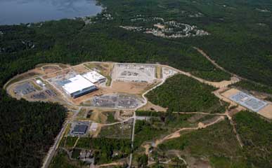
To be clear, AMD had no plans at that time to build a new fab in New York or anywhere else. But with that one cold call, and four years later, New York had the deal on the largest private economic development project in its history. The GLOBALFOUNDRIES* project will result in the construction of a $4.2 billion semiconductor manufacturing facility, called Fab 8, at the Luther Forest Technology Campus and the creation of 1,465 new high-tech jobs in New York. It will also solidify the state's position as a global high-tech center. The lessons learned from this project can add value to any site selection process.
New York's Approach - Make Them an Offer They Can't Refuse
In the late 1990s, New York adopted a new economic development strategy with an impressive goal: to attract a major semiconductor manufacturer to the state - not just any manufacturer, but an industry leader whose presence would spur the development of an entire semiconductor industry cluster. The new strategy was designed to help replace New York's declining manufacturing industries with the high-tech, high-value jobs of the future. According to Dennis Brobston, President of SEDC, "Our state and regional leaders chose to focus on a semiconductor industry strategy for the transformative effect it could have on the economy and for the opportunities it would afford us in the future. We knew there were hard work and investment and risk ahead of us, but firmly believed we had the partners and assets needed to be successful."
New York's team did its homework. A strong development team with representatives from the public, private, and academic sectors worked together. Industry experts were consulted so the team would better understand the semiconductor industry and could identify the companies that would most benefit from New York's assets. The team visited the Dresden semiconductor cluster and learned about the type of incentives the State of Saxony and German governments gave to semiconductor manufacturers. SEDC identified an ideal site for semiconductor manufacturing and worked to make it shovel-ready with financing from local partners such as the Adirondack Trust Company. State and local governments began needed infrastructure improvements, and state leaders committed to negotiating a competitive incentive package when the time came.
New York believed that AMD was a perfect candidate for its pitch, and AMD agreed to New York's request for a meeting. By all measures, New York's cold call was a success. When describing the initial meeting, Terry Caudell, who led AMD's site selection process and is currently Project Manager for the GLOBALFOUNDRIES Fab 8 project says, "They [the New York team] felt that AMD was a primary candidate for the semiconductor assets and resources that New York had put in place. They presented an opportunity to us that we felt was unique, and we made the decision then to further explore whether New York fit into AMD's long-term capacity strategy."
Initial interest led to a site visit so AMD could learn more about the region. A full spectrum of community partners participated in the site visit to give AMD a complete picture of the assets in place to support a new fab. Team members included state and local elected leaders; local public agencies like the Saratoga County Water and Sewer authorities; private partners such as SEDC, the Center for Economic Growth (CEG), and National Grid; and academic partners including the College for Nanoscale Science and Engineering (CNSE) and Hudson Valley Community College (HVCC). The visit convinced AMD it should move to the next step. Says Caudell, "Our first exposure to all of the pre-development work done at the Luther Forest Technology Campus was impressive. We looked at this site in context of the work we had already done in Dresden and went away feeling that this team had done its homework."
Site Selection Begins in Earnest
After visiting New York, AMD initiated its formal site selection process. AMD did not settle on New York immediately, but approached its potential capacity expansion from a global perspective. Every region with a 300-mm factory was evaluated against several criteria including economics, labor, education, utilities, political stability, cost of manufacturing, and availability of capital. The resulting short list included three regions: Dresden, Germany; Singapore; and New York.
In parallel with its global search, AMD also evaluated 10 New York sites with the potential to support a high-tech industry cluster. The Luther Forest Technology Campus stood out as the clear winner. The campus, located 20 minutes north of the Albany, is a 1,014-acre greenfield site with few wetlands. The region is home to a highly skilled work force and has nearby R&D assets like IBM's research park in Fishkill, the College of Nanoscale Science and Engineering at the University at Albany, and the International Sematech Consortium. It's close to major transportation routes, and utility companies had already developed plans to build the advanced utility infrastructure at the campus.
The final piece of the puzzle was the development of a comprehensive cost model to predict the true cost of manufacturing in each region around the world. The model factored in construction costs, utility costs, local labor rates, and potential benefit packages, and provided a realistic cost per wafer estimate in each location. The cost model turned out to be a critical tool that helped both AMD and New York understand what type of incentive package would make New York globally competitive. New York simply had to commit to an incentive that brought the cost of manufacturing in the state in line with the cost of manufacturing in Singapore or Germany. Would New York be prepared to offer AMD such a deal? NY's Innovative Investment Package
In June 2006, a year after the New York team first visited Austin, both New York and AMD issued their first commitment to the project. AMD announced the results of its site selection process, and the Luther Forest Technology Campus was named as the best global location for its potential capacity expansion. New York agreed to commit to a $1.2 billion incentive package, and AMD signed a letter of intent confirming that it would build in New York if it indeed went ahead with a new fab. The incentive package that New York offered was unique in one very important way - it built in the time and flexibility that AMD needed to work out the details of its expansion. From the time the letter of intent was signed, AMD had a two-year period in which it could exercise the incentive package option.
Says Travis Bullard, GLOBALFOUNDRIES Public Affairs and Communications Manager, and a member of the original AMD site selection team, "There is so much investment that goes into bringing one of these facilities on line; New York's willingness to engineer flexibility into its benefit package gave AMD the time it needed to move forward."
In this instance, the details were more important than anyone originally imagined. In the end, AMD made the strategic decision to spin off its manufacturing assets to a new company, GLOBALFOUNDRIES, which will own and operate Fab 8.* There has been much talk about the magnitude of the incentive package that New York offered to AMD. Indeed, this incentive is the largest private economic development project in the state's history. The simple fact is that this innovative investment brought the cost of building and manufacturing in New York in line with other regions of the world. Says Brobston, "If regions are serious about reversing the flow of high-tech jobs to other countries, then their incentives must create a level playing field for global companies. New York's incentive was a strategic investment designed to lure an economic driver that would spur significant job growth and solidify our state's position as a premier global technology hub."
Lessons Learned
The site selection process is now complete and GLOBALFOUNDRIES' Fab 8, a 1.3 million-square-foot manufacturing facility, is on schedule to begin production in 2012. For AMD/GLOBALFOUNDRIES, two key factors set New York apart from the rest: the state's clear strategic vision and community preparedness.
Says Bullard, "When you look at why this process was successful, I think the answer is that [the state] knew exactly what it wanted. New York State and this area [Saratoga County] in particular determined that they wanted to bring a semiconductor chip fab here. What you are seeing here today is the result of New York setting a goal and identifying the resources needed to be in place to make the decision for AMD so much easier."
Will New York's investment pay off? New York's leaders believe that the presence of GLOBALFOUNDRIES in Saratoga County - along with the many other regional assets like IBM, GE, SEMATECH, CNSE, and other research leaders - will cement the region's position as a premier global nanotech center. The industry seems to have taken notice, and the industry (including SEMATECH and MW+ US Group) has begun to move its operations to New York. SEDC continues to work with companies in the nanotech, biotech, and cleantech industries to fill the remaining two million square feet of developable space at the Luther Forest Technology Campus. Without a doubt, the GLOBALFOUNDRIES project will positively impact the New York economy for years to come.
*Note: When this project began, GLOBALFOUNDRIES did not exist. During its capacity expansion decision-making process, and as part of its Asset Smart strategy, AMD divested itself of all manufacturing operations. GLOBALFOUNDRIES was established in March 2009 after AMD spun off its manufacturing unit in a joint venture with Abu Dhabi's Advanced Technology Investment Co. (ATIC). GLOBALFOUNDRIES will build chips for both AMD and other third-party customers. The incentive package that New York committed to AMD was transferred to GLOBALFOUNDRIES.
Recent Project Announcements
Scout Space Expands Fairfax County, Virginia, Production Operations
06/15/2026
CRP Automotive Plans Pittsfield, Michigan, Operations
06/15/2026
Faith Technologies Plans Monroe, Louisiana, Manufacturing Operations
06/15/2026
Front Line Safety Plans Kansas City, Missouri, Distribution Operations
06/14/2026
Durango Machining Innovations Plans Farmington, New Mexico, Operations
06/14/2026
West Fraser Expands McDavid, Florida, Sawmill Operations
06/14/2026
Alstom Plans Newark, Delaware, Operations
06/14/2026
Janicki Industries Plans Great Falls, Montana, Manufacturing Operations
06/13/2026
Urban Outfitters Plans Bucks County, Pennsylvania, Operations
06/13/2026
Raytheon Expands Portsmouth, Rhode Island, Missile Defense Operations
06/13/2026
Luxembourg-Based ArcelorMittal Building Solutions Plans Macon-Bibb County, Operations
06/13/2026
South Korean-Based Kamtec Auto USA Plans Auburn, Alabama, Manufacturing Operations
06/12/2026
NovaSpark Energy Expands West Monroe-Establishes Houma, Louisiana, Operations
06/11/2026
Austria-Based Mosdorfer Plans Oconee, South Carolina, Manufacturing Operations
06/11/2026
Most Read
-
Where Early-Stage Life Sciences Companies Get Stuck Scaling Their Real Estate—and How to Move Forward
Q2 2026
-
Where Workforce Capacity Is Being Built — and Where It’s Being Deployed
Q1 2026
-
40th Annual Corporate and 22nd Annual Consultant Site Selection Survey Results
Q1 2026
-
2025’s Top States for Business: How the Winners Are Outpacing the Rest
Q3 2025
-
The Workforce Bottleneck in America’s Manufacturing Revival
Q4 2025
-
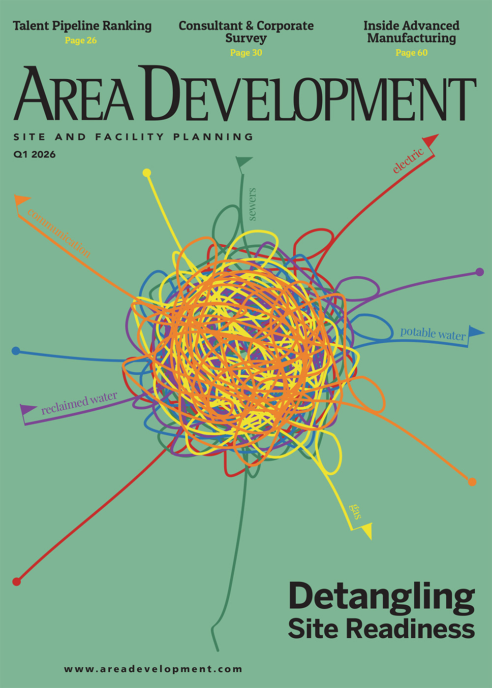
What Does “Site Readiness” Really Mean?
Q1 2026
-
Phillip Morris International Starting Building Before Plans
Q1 2026