The U.S. CHIPS and Science Act—signed into law in 2022 and aimed at reviving America’s domestic manufacturing sector—has so far resulted in $29 billion worth of deals with eight manufacturers for projects across 11 states. Add the $450 billion of private investments for 80 projects across 25 states inspired by the CHIPS Act, and the United States is well on its way to reclaiming its position as a leader in semiconductor manufacturing.
“America invented these chips, but over time, we went from producing 40% of the world’s capacity to just over 10%, and none of the most advanced chips,” President Biden has repeatedly stated.
That’s about to change. The billions of dollars companies and investors are pouring into this industry is expected to lead to a 203 percent surge in U.S. fabricating capacity by 2032, according to a new report from by the Semiconductor Industry Association (SIA) and the Boston Consulting Group (BCG) entitled Emerging Resilience in the Semiconductor Supply Chain. On top of that, advanced chip production in the United States is forecast to jump 28% by 2032, compared with 0% in 2022.
That will undoubtedly create thousands of new jobs and boost the economy.
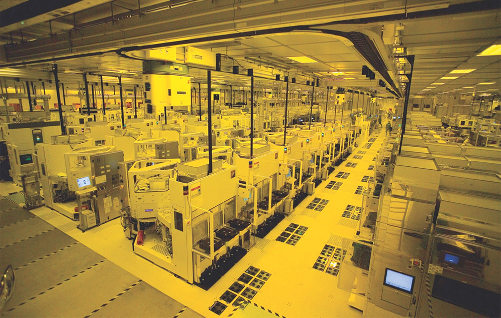
But semiconductor manufacturing is a thirsty business—using millions of gallons of water per day—and many of these projects to build or expand facilities are in water-stressed regions in states like Arizona and Texas.
To put it in perspective, one person uses around 80 gallons of water per day, on average. A fabrication plant can use up to 10 million gallons of water per day, depending on the size of the plant and type of chip being produced. That’s nearly equivalent to the water needs of a small city like Santa Clara, California, which has a population of 126,215.
Chipmakers around the world are already consuming as much water as Hong Kong, a city with a population of 7.5 million, according to analysts at S&P Global Ratings.
10 million gallons per day -- that's the amount of water it takes to operate a semiconductor fabrication plant, nearly equivalent to the water needs of a small city like Santa Clara, California. Advanced chips power everything from the latest iPhone to electric vehicles, medical devices, high performance computing (HPC), and devices powered by Artificial Intelligence (AI). As technology continues to become more sophisticated, demand for more advanced chips will grow, which, in turn, will lead to an increase in water demand.
Just last year, more than one trillion semiconductors were sold around the world, according to the SIA. And that figure is expected to continue to grow. Having a steady water supply to meet that demand will remain top of mind.
“We view water scarcity as a risk in the coming decade for the tech hardware industry, particularly the water-intensive semiconductor subsector,” the S&P analysts wrote.
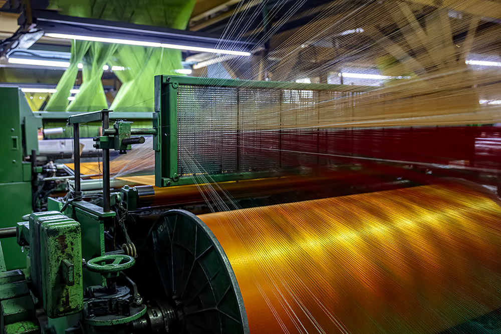
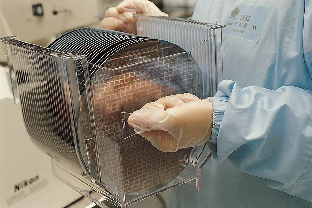
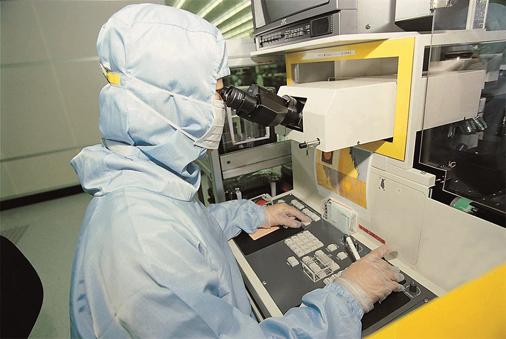
That’s because advanced chip production uses ultrapure water (UPW)—highly refined fresh water—to clean and purify wafers. These wafers will typically go through a several-step process and UPW is used each time so the more advanced they become, the more processing they need. Water is also used to cool machines and for general use.
Taiwan Semiconductor Manufacturing Company (TSMC), which makes 90 percent of the world’s advanced chips, reported that the annual capacity for its manufacturing facilities and its subsidiaries exceeded 16 million 12-inch equivalent wafers in 2023.
“The semiconductor sector is on track to increase water consumption by a mid to high-single-digit percent each year, driven by capacity expansion and the demands of advancing process technology,” according to S&P analysts.
TSMC also said it continued to implement four major water saving measures throughout its operations in 2022: reducing facility system water consumption, increasing the wastewater recycling of facilities, improving the water production rate of the system, and decreasing water discharge loss from the system.
Still, the renewed resurgence of water intensive semiconductor manufacturing in the United States begs the question: Where will the water come from?
Take Arizona, for example. Two of the largest manufacturers—TSMC and Intel—are growing their footprints in and around Phoenix, a city that’s not considered a water oasis. But the advantage, say city officials, is that “desert cities know that drought is a constant threat and plan accordingly.” It’s that type of planning that has helped Phoenix make it through every drought without any major water restrictions.
Manufacturers and local municipalities continue to work closely together to address the anticipated increase in water demand and infrastructure needs.
In 2020, TSMC signed a $12 billion agreement to build its first U.S. fabrication plant in Phoenix. In exchange, the city committed to spending $205 million in infrastructure improvements to support the project, comprising three miles of full arterial streets including streets, curb, gutter, sidewalk, streetlights and landscaping, new regional public water infrastructure improvements, and new public wastewater infrastructure improvements.
35 billion gallons -- that's the amount of ultrapure water (UPW) used throughout Taiwan Semiconductor Manufacturing Company's global operations in 2022, marking a 21 percent increase from the previous year. More recently TSMC announced it was building two more fabs and modernizing existing facilities in Arizona, helped by a $6.6 billion investment under the CHIPS Act.
The first fab, which is expected to start production in 2025, will leverage 4nm technology and produce 20,000 wafers per month. The second fab, expected to start production in 2028, will produce the most advanced 2nm technology alongside 3nm technology. The third, most recently announced fab, is slated to produce chips using 2nm or even more advanced processes by the end of the decade.
In total, TSMC is investing $65 billion in Phoenix, making it the largest foreign direct investment in Arizona, and the largest foreign direct investment in a greenfield project in the United States.
“By increasing our capacity for leading-edge technology in Arizona, we will enable our customers to unleash innovations across mobile, AI and HPC applications for all industry sectors,” TSMC stated.
Meanwhile, Intel has been in the state since 1979, with four fabs operating and two more on the way. The chipmaker has committed $32 billion to build those new fabs, as well as modernize an existing one in Chandler (near Phoenix), where it will produce advanced logic chips used in a number of different U.S. industries, including automotive, medical device and aerospace. Intel will receive up to $8.5 billion under the CHIPS Act to help fund the Arizona projects, as well as modernize packaging facilities in New Mexico, expand R&D in Oregon and built two new fab plants in Ohio.
“We work very closely with local officials in all the communities in which we operate, including the City of Phoenix Water Department,” said a TSMC spokesperson. The company is focusing on recycling and reclamation at its Arizona site with roughly 65 percent of the water at the first fab plant coming from its in-house recycling systems at startup. The recycled water will be used in air scrubbers and cooling tower systems.
On the reclamation side, TSMC is working toward 90 percent water reclamation by building an advanced water treatment facility to achieve ‘near zero liquid discharge.’ “This means the fabs will be capable of reusing nearly every drop of water back into the facility,” said the spokesperson.
The company says it is always looking for ways to be more efficient about its water usage, which includes wastewater and byproduct treatment. The spokesperson noted that TSMC has invested considerable effort into building a comprehensive wastewater treatment system, a water reclamation system, and a waste material recycling system to reduce water consumption, decrease wastewater discharge and increase overall water efficiency.
The semiconductor sector is on track to increase water consumption by a mid to high-single-digit percent each year, driven by capacity expansion and the demands of advancing process technology. Furthermore, as part of its effort to reduce total water usage, TSMC's discharged water is graded by purity, said the spokesperson with the cleanest being reused in the manufacturing process. The second grade will be used in other ways such as cooling-tower water. And finally, wastewater that cannot be recycled will be discharged to treatment facilities for final wastewater treatment. The spokesperson also noted that all tap water used at TSMC is completely reclaimed every day through layers of recycling, and that each drop of water is used an average of 3.5 times.
Meanwhile, Intel has a goal to achieve net positive water by 2030. Net positive is defined as water returned through water management practices plus water restored to local watersheds for more than 100% of its freshwater consumption.
To meet this goal, the chipmaker is taking a three-pronged approach: reducing its water footprint through innovative conservation projects, treating water to reuse within its operations, and working with local communities to restore water to watersheds.
In Arizona, Intel has created 21 water restoration projects that are already achieving net positive water. The chipmaker has also restored 1.7 billion gallons of water and treated more than 14.5 million gallons of water per day at its 12-acre on-site water reclamation facility and the Ocotillo Brine Reduction Facility, a partnership with the city of Chandler.
The Arizona Department of Water Resources has already been investing in water conservation and reuse. In fact, Arizona has already stored nearly 3 trillion gallons of water in underground aquifers should it face a water crunch. That’s enough to supply the city of Phoenix for 30 years.
However, these are widely known issues and, much like your stock portfolio, Arizona’s state agencies have taken a diversified approach to water management. In addition to the Colorado River, Arizonians get water supply from groundwater (41 percent), in-state rivers (18 percent), and reclamation (5 percent).
Earlier this year, the Phoenix City Council announced plans to reopen and expand the Cave Creek Water Reclamation Plant, which was shuttered in 2009 due to an economic slowdown. The plant, which is expected to be operational by the end of 2026, could eventually produce 6.7 million gallons of potable water a day—enough to supply 25,000 households a year.
"Phoenix takes seriously the need to secure our water future and continues to bring new solutions to the table to do so," said Phoenix Mayor Kate Gallego.
Ohio is another state attracting attention from chipmakers. Intel is investing more than $28 billion to build two new fab plants at a site just outside of Columbus that will produce advanced chips. The Ohio mega site, known as Ohio One, is in the city of New Albany and will span 1,000 acres—enough to accommodate eight plants.
So, where will the water for these new fabs come from? Intel says New Albany will supply the water, which originates from the Hoover Reservoir along Big Walnut Creek. Intel will treat the water onsite at its own water system that will have the capacity to process millions of gallons of water daily and create UPW that will be used to process the wafers as part of the chipmaking process.
Intel plans to take that water, after it’s been used in the manufacturing process and treat it for reuse in multiple ways at its mega site before treating it again to meet approved water quality standards and discharged into the sanitary sewer system, where it will be treated at the Columbus city wastewater treatment plant.
We found that corporations are pursuing multiple pathways to address water stress, including funding on-the-ground water projects, improving water management in their owned and operated facilities, using their brand to raise awareness about water challenges, and developing innovative products and services. Intel has firmly stated that there will not be any direct wastewater discharges from its manufacturing facilities. The only permissible discharge will be stormwater and even that will be diverted first into retention basins that are designed to manage runoff by storing stormwater and releasing it on a gradual basis to prevent flooding and erosion.
The chipmaker is also investing in a water restoration project near Dillon Lake, located in the Licking River watershed near the chipmaker’s Ohio One campus. The project will convert roughly 90 acres of cropland into a wetland and floodplain treatment plain that will reconnect the lake to the Licking River, reduce sediment and nutrient loading to Dillon Lake. Ultimately, Intel’s share of this project is expected to restore about 27 million gallons of water annually.
“More than 10 years ago, we began to explore how we could better understand and reduce our water footprint. Five years ago, we set a public goal to restore 100 percent of our consumption and became the first tech company to set a companywide water restoration goal,” said Todd Brady, Intel chief sustainability officer and vice president of Global Public Affairs, in a statement.
According to its most recent Corporate Responsibility Report, Intel said it conserved approximately 10.2 billion gallons of water last year in all of its operations and through community collaborations, as well as enabling the restoration of 3.1 billion gallons of water through watershed restoration projects. The chipmaker said it maintained net positive water in the United States and India in 2023 and reached net positive water in Costa Rica and Mexico.
Meanwhile, Samsung, which was awarded $6.4 billion under the CHIPS Act, has plans to build leading edge logic, R&D and advanced packaging fabs in Taylor, Texas, as well as expand its current-generation and mature-node facility in Austin, where Samsung Semiconductor has been operating two fab plants since 1996. With the additional funding, Samsung plans to invest more than $40 billion in the region.
Samsung Semiconductor Chief Executive Kye Hyun Kyung said in a statement that the chipmaker is committed to implementing sustainable water resource management technologies, pledging to boost water recycling rates and purifying discharged water.
“Our water strategy is focused on conserving water in our operations, collaborating with our community and creating programs to proactively prevent pollution and expertly manage wastewater discharge,” said Michele Glaze, Director of Communications, Samsung Austin Semiconductor, adding that the new fab being built in Taylor will have a minimal impact on the environment. “The primary water for Taylor will be groundwater that should not tax the existing surface water sources that municipalities use.”
Glaze said that the city of Taylor will supply the domestic water, which is used for daily personal use such as drinking, food prep and flushing toilets, while private utility firm Epcor will supply the industrial water, which will be used for washing, cooling, processing, and fabricating. In other words, Epcor will be supplying most of the water needed for processing Samsung’s wafers.
It’s not clear how much water Epcor will be supplying but it’s been widely reported that it will come via pipeline from the Carrizo-Wilcox Aquifer in Milam County. The aquifer is the third most important groundwater resource in Texas, according to a report from Texas A&M AgriLife, which also noted that the aquifer’s water table has dropped more than 150 feet over the past several decades as recharge rates appear to have slowed, possibly due to changes in land use that may have created unfavorable conditions.
“The target is to reclaim or reuse 75 percent of the process water within the fabrication facility, with the balance purified and returned to the environment to help sustain the natural water cycle and support the local ecosystem,” Epcor said in a statement.
What about climate change? That’s a wild card that semiconductor manufacturers and the regions in which they are growing are already contending with and will continue to do so well into the future.
“Climate change is testing chipmakers,” noted the S&P analysts, adding that it is already “raising the rate of extreme weather, the frequency of drought, and the volatility of precipitation, limiting chipmakers' ability to manage production stability.”
As semiconductor processing technology advances, there will be greater demand for water, and particularly UPW. It brings us back to the central question around where will the water come from?
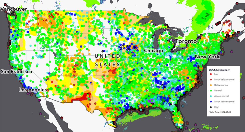
The Colorado River is a notable example of the unpredictability of the effects of climate change. While the river basin is among the most water stressed in the world, it’s future may not be as dire as some may have thought. The river supports the water needs of seven states—Arizona, California, Colorado, Nevada, New Mexico, Utah, and Wyoming—and Mexico. The Colorado is also among the most tightly regulated and managed, with a system of dams, reservoirs, and pumps in the lower basin designed to capture and store and supply water.
However, warming temperatures created multi-decade drought conditions and raised concerns about more reductions in water flow, according to researchers at the Pacific Institute, a global water think tank.
“The combination of a crippling drought that began 24 years ago, the historic over-allocation of the river’s declining runoff, and climate change have exacerbated a structural deficit—where more water leaves the system than enters it,” wrote Pacific Institute researchers Dr. Christine Curtis, Cora Snyder, and Michael Cohen in a report entitled Pathways and Barriers to Corporate Water Stewardship in the Colorado River Basin.
As state agencies, policymakers and corporations continue to work on water mitigation plans, researchers at the Cooperative Institute for Research in Environmental Sciences (CIRES) at the University of Colorado Boulder suggest there may be less of an issue than previously thought when it comes to precipitation, which feeds into the river flow.
Using various climate modeling and working alongside analysts at other institutions, the CIRES researchers, who published their findings in the May 1, 2024, issue of the Journal of Climate, noted that “precipitation falling in the river’s headwaters region is likely to be more abundant than during the prior two decades.”
According to their research, which included analyzing data back as far as 1895, precipitation in the headwater region, which provides 85 percent of the water that flows through the Colorado River, should remain high enough to help offset the negative impact of rising temperatures due to climate change.
It's not just Mother Nature who has a role to play in mitigating water stress.
“Despite the brief reprieve provided by last winter’s exceptional snowpack, we still need all hands on deck, from everyone who depends on Colorado River water, to lean in and help get the system into balance,” noted Curtis, Snyder, and Cohen.
Semiconductor manufacturers are being proactive to ensure they are helping and not hindering the environment in which they operate.
“We found that corporations are pursuing multiple pathways to address water stress, including funding on-the-ground water projects, improving water management in their owned and operated facilities, using their brand to raise awareness about water challenges, and developing innovative products and services,” said Curtis, Snyder, and Cohen. The Pacific Institute researchers held 20 interviews with corporate and non-corporate stakeholders as part of their research.
TSMC, for example, is no stranger to nature’s twists and turns. In 2021, just as the U.S. federal government declared a shortage at the Colorado River for the first time ever, due to drought conditions, Taiwan experienced its worst drought in half a century. TSMC managed to keep its Taiwan operations running without disruption, thanks to having a detailed response plan in place designed to handle water shortages at different stages.
“Increasing TSMC’s resilience against natural events—such as drought—is a regular focus,” said the company spokesperson, noting that TSMC was the first semiconductor manufacturer to receive the highest certification, known as the Platinum certification, from the Alliance for Water Stewardship (AWS) for its commitment to and implementation of sustainable water management.
AWS, a global membership organization comprising businesses, nonprofits, and the public sector, promotes “the use of water that is socially equitable, environmentally sustainable and economically beneficial.” Achieving an AWS standard signals a company’s commitment to sustainable water management.
Intel was the second to earn Platinum certification from AWS for its Ocotillo, Arizona Campus in Chandler. “With our proactive efforts, we seek to mitigate climate and water impacts,” Intel stated in its Corporate Responsibility report.
Those efforts include nine projects along the Colorado River, four along the Verde River basin and seven others that feed into Arizona. In all, these projects are expected to restore nearly 2.2 billion gallons of water per year to the state, once fully implemented.
Even with all this planning, the relationship between semiconductor manufacturers and water supply remains a fragile one. Apart from Intel’s Ohio facility, the remaining six planned across the United States are situated in watersheds classified as at high- or extremely high risk of water stress, according to an analysis by Josh Lepawsky, a geography professor at Memorial University of Newfoundland and Labrador.
On the bright side, companies like Intel and TSMC “are making impressive progress in water use reduction techniques,” writes Lepawksy. Still, that may not be enough to combat the effects of climate change.
“No matter how dramatic those ductions are, they cannot create a situation in which the water needed for semiconductor manufacturing is simultaneously accessible to other water users,” Lepawsky notes, adding that without a steady, and stable, supply of large amounts of water, there will be no semiconductors and without semiconductors there will be no electronics. Stay tuned.